热销产品
IGBT模块尖峰电压测量及吸收电容规格
目录
General 概述
Capacitor parameter 电容参数
DC voltage class 直流电压等级
Capacitance and series-inductance 电容和串联电感
Pulse handling 脉冲处理
RMS voltage and RMS current 有效值电压及有效电流
Lifetime 寿命
Measurements and verification 测量与验证
Voltage stress of IGBT (VCEpeak) IGBT的电压应力
Measuring capacitor RMS current 测量电容有效电流值
Temperature and self heating under operation 运行时温度及自加热
Symbols and terms used 符号与术语
本应用手册阐述了在大功率应用场合,如何为IGBT模块选择及测试吸收电容以及如何测试效果。可以帮助防止IGBT模块及吸收电容的电气或热过载造成的失效,本文同时分析了电容的哪个参数应该需要关注,及如何实施必要的测试。文章来源:http://www.igbt8.com/il/250.htmlCapacitor parameter 电容参数
DC voltage class 直流电压等级
Capacitance and series-inductance 电容和串联电感
Pulse handling 脉冲处理
RMS voltage and RMS current 有效值电压及有效电流
Lifetime 寿命
Measurements and verification 测量与验证
Voltage stress of IGBT (VCEpeak) IGBT的电压应力
Measuring capacitor RMS current 测量电容有效电流值
Temperature and self heating under operation 运行时温度及自加热
Symbols and terms used 符号与术语
General
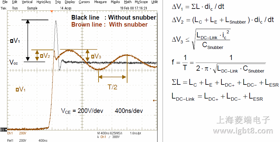
If high currents are switched fast, then voltage overshoots occur, which can destroy the switching power semiconductor. The voltage overshoot is caused by the energy stored in the magnetic field of the current path (e.g. DC-link connections). It is linked by the value of the parasitic inductance or stray inductance LS (E=0,5*LS*i²). The voltage (V=LS*di/dt) may exceed the maximum blocking voltage of the power semiconductor (VCES, VRRM…) because it is added to the DC-link voltage.
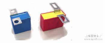
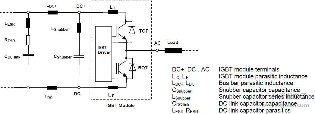
The first countermeasure is a good low inductive DC-link design to keep the voltage on the semiconductor low. This is done by means of a laminated bus bar system (sandwich of +DC, –DC metal sheets and an insulation layer between) and short connections between the voltage source (DC-link capacitor) and power semiconductor. In addition, snubber capacitors are recommended, which should be mounted directly on the DC-link terminals of each IGBT module. This snubber works as a low-pass filter and “takes over” the voltage overshoot. Fig. 1 shows typical designs. The waveform in Fig. 2 shows in comparison the voltage across an IGBT at turn-off with and without snubber capacitor. The effect of voltage spike reduction can be seen clearly. Fig. 3 shows an equivalent circuit with parasitic inductances.
上海菱端电子科技有限公司:
联系人:夏小姐
服务热线:021-58979561
业务咨询qq:447495955
业务咨询qq:1852433657
业务咨询qq:513845646
技术支持qq:313548578
技术交流群:376450741
业务咨询:
业务咨询:
业务咨询:
技术支持:
媒体合作:
Fig. 1 Low inductance snubber capacitors for mounting on IGBT modules
In order to decide whether a snubber capacitor is necessary, the maximum collector-emitter voltage (VCEpeak) of the IGBT has to be checked under worst case conditions to be sure that VCES will not be exceeded under any operating condition. If necessary, several aspects have to be considered when choosing the right snubber capacitor for the application:
1. Capacitor DC-voltage class.
2. Capacitance value and series inductance
3. Pulse handling capability.
4. RMS voltage and RMS current
5. Lifetime
Fig. 2 Typical waveform of VCE voltage on IGBT at switching off
Fig. 3 Equivalent circuit diagram of IGBT module connected to DC-link and snubber capacitor
Capacitor parameter
DC voltage class
The maximum continuously applied DC voltage can be the rated DC voltage given in the data sheet to achieve the life expectancy. Semiconductors with 1200V blocking voltage are used with up to 900V DC-link voltage. For these applications, capacitors with a rated voltage of 1000V are recommended. For 1700V semiconductors, 1250V or 1600V capacitors are recommended, depending on the DC-link voltage.
The peak voltage also has to be in the admissible values because otherwise the plastic film could be damaged. Permissible peak voltages are given in the data sheets or have to be requested. Consider also that the applied DC voltage has to be derated when the capacitor is operating at higher temperatures than the rated temperature.
Capacitance and series-inductance
Capacitance and series-inductance
The capacitance value has to be high enough to achieve sufficient voltage spike suppression during switching off. Typical values for these capacitors are from 0.1 μF to 1.0μF. But not only is the capacitance value important for this. Also a low inductive design of the capacitor isimportant. The remaining inductance, caused by the loop between the terminals and the internal connections of the capacitors is responsible for the first voltage spike V2 seen in Fig. 2. A high capacitance value is no guarantee for a low voltage spike if the self-inductance remains. A low self-inductance can be achieved by using capacitors with wide flat terminals that can be screwed directly onto the IGBT module terminals. The capacitor should be designed so that the terminals encircle as small an area as possible and that they are directly connected to the capacitor coil without having internal wires between (see Fig. 1). The choice of the correct snubber should be determined by measurements. Furthermore, metallized polypropylene foil capacitors should be used with plastic case according to UL94V-0.
Pulse handling
The inner connections of the capacitor are capable of withstanding only a limited amount of energy at each switching event. The data sheets of the supplier specify limits for pulse operation as i²t or v²t values. These values can be calculated from the oscillating current or voltage waveform of the capacitor. This calculation can easily be carried out using modern digital oscilloscopes.
A capacitor failure can occur only because of very high peak currents, even when the involved voltages are lower than the specified ones. In this situation the critical thing is the involved energy and normally there will be a loss of connection between metal spray and film metallization. Because of the very high energy involved the film metallization will be vaporized on the connection area to the metal spray. This will lead the capacitor to a high loss factor or even to a capacitance loss. The maximum dv/dt values are less critical because of the damped sinusoidal waveform.
RMS voltage and RMS current
A damped oscillation occurs at each switching event (on or off = twice switching frequency of the IGBT) between the snubber capacitor and the bus bar capacitance. The maximum magnitude, V3, for an undamped oscillation and the frequency can be calculated using the formulae in Fig. 3. This RMS current leads to self heating of the capacitor. The capacitor will stabilize at a certain temperature which also depends on the ambient temperature and on the mounting conditions (e.g. temperature of power module terminals).
Data sheets give values for the permissible RMS current and RMS voltage depending on the frequency. The oscillating frequency depends on the DC-link stray inductance and the snubber capacitor value. Typical values are in the range of 100 kHz to 1 MHz. The permissible RMS current decreases with the frequency because the losses increase.
Please see chapter “Measuring capacitor RMS current” which gives tips for practical current measurement on the capacitor.
Lifetime
The capacitor lifetime and failure rate is mainly affected by the operating temperature and operating voltage. The failure criteria differ from supplier to supplier. Check the data sheet and application notes for lifetime and failure rate data.
Self healing
The most important reliability feature of film capacitors is their property to self-heal that means to clear a defect in the dielectric. The capacitor can be used afterwards without any restrictions. This defect is caused when the dielectric breakdown field strength is exceeded locally at a weak point in the foil.
The most important reliability feature of film capacitors is their property to self-heal that means to clear a defect in the dielectric. The capacitor can be used afterwards without any restrictions. This defect is caused when the dielectric breakdown field strength is exceeded locally at a weak point in the foil.
服务热线:021-58979561
业务咨询qq:447495955
业务咨询qq:1852433657
业务咨询qq:513845646
技术支持qq:313548578
技术交流群:376450741
业务咨询:
业务咨询:
业务咨询:
技术支持:
媒体合作:
沪ICP备09068927号 igbt8.com版权所有 Copyright 2008-2018
URL:http://www.igbt8.com qq:1852433657 欢迎加入IGBT技术交流群:376450741
技术支持: IGBT应用技术网
URL:http://www.igbt8.com qq:1852433657 欢迎加入IGBT技术交流群:376450741
技术支持: IGBT应用技术网